
Company News
Joint Research by Liaocheng University, Shenzhen University and Shenzhen Technology University Published in Advanced Optical Materials Uses Prismlab Micro/Nano 3D Printing for Room-Temperature High-Performance Terahertz Detection and Modulation
The pursuit of faster communication has never stopped. As 5G becomes widely deployed, next-generation 6G communication is turning toward the terahertz band - often described as the last largely untapped region of the electromagnetic spectrum - with the potential to enable ultra-high data rates, ultra-low latency, and ultra-dense connectivity. However, terahertz technology has long faced two major barriers: achieving high-sensitivity detection at room temperature and realizing dynamic, efficient modulation. The combination of Weyl semimetals, three-dimensional micro/nano structures, and the sub-pixel micro-scanning 3D printing technology of Shanghai Prismlab Technology Co., Ltd. ("Prismlab") has now provided a new route forward.
The research, jointly completed by Liaocheng University, Shenzhen University, and Shenzhen Technology University in China, was published in the internationally renowned journal Advanced Optical Materials under the title Optical and Magnetic Field Modulated CrGeTe3/Co3Sn2S2 Nanofilm Covered Metamaterials Fabricated by Sub-Pixel Micro-Scanning 3D Printing for 6G Applications. In the study, the team used Prismlab's sub-pixel micro-scanning 3D printing technology to fabricate three-dimensional microstructures with localized surface plasmon enhancement, providing critical manufacturing support for core 6G devices.

From Materials to Structures: Three Breakthroughs in Terahertz Devices
The terahertz band has low photon energy and is difficult to integrate with the operating mechanisms of conventional electronic and photonic devices. As a result, high-performance terahertz functional devices have long been lacking. Existing terahertz detectors either require low-temperature operation or offer insufficient sensitivity, making it difficult to meet the stringent requirements of 6G communications.
The breakthrough of this study lies in a three-way synergy of materials, structure, and process:
Material combination: a heterojunction was constructed by combining the magnetic Weyl semimetal Co3Sn2S2, which offers high carrier density and room-temperature magnetic response, with the quasi-two-dimensional van der Waals ferromagnetic semiconductor CrGeTe3, which provides strong terahertz absorption. This design integrates photoelectric and magnetoelectric properties.
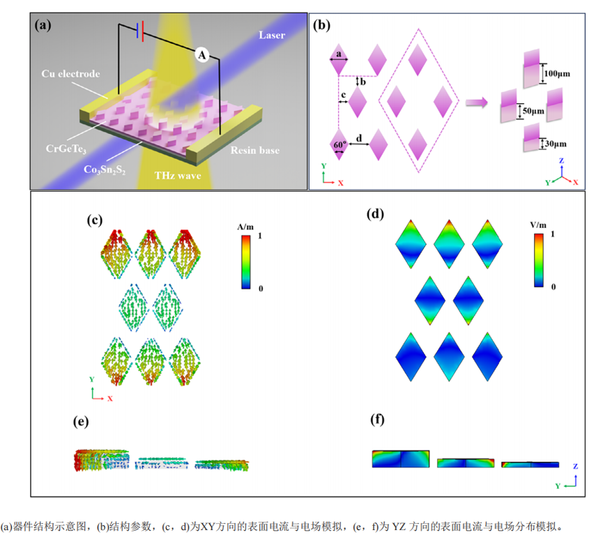
Three-dimensional microstructure: a subwavelength diamond-shaped microarray was designed to highly localize terahertz field energy through localized surface plasmon effects. A Fabry-Perot-like cavity structure along the Z direction further extends the optical path and significantly enhances light-matter interaction.
Manufacturing process: Prismlab's sub-pixel micro-scanning 3D printing technology was used to precisely realize cross-scale fabrication of complex three-dimensional microstructures.
Prismlab 3D Printing: Accurately Translating Complex Microstructures into Physical Devices
The successful implementation of this technology relies on the key support of Prismlab's sub-pixel micro-scanning 3D printing equipment. Using this technology, the research team fabricated three-dimensional microstructures with staggered diamond arrays, featuring a structural feature size of 50 microns, a staggered spacing of 25 microns, and an overall effective detection area of 10 x 10 mm^2.
Traditional microstructure fabrication relies on photolithography, molds, and related processes, making it difficult to flexibly design high-aspect-ratio, complex three-dimensional structures. These methods are also time-consuming and costly. Prismlab's sub-pixel micro-scanning technology breaks through these limitations:
2-micron precision: a microlens array reduces the beam to a sub-pixel-level spot, while piezoelectric ceramic micro-vibration scanning enables the precise curing and forming of ultra-fine patterns.
High-aspect-ratio fabrication capability: 2-micron layer thickness processing supports complex three-dimensional structures and meets the stringent morphology requirements of terahertz devices.
Mold-free rapid iteration: from design to forming, the process can be completed in just a few hours without molds, supporting rapid optimization of structural parameters.
This combination of precision and design freedom enabled the accurate realization of the diamond microarray described in the paper. The tip curvature, edge contour, and Z-direction stretching ratio were precisely reproduced, ensuring stable localized surface plasmon performance.
Broad Application Prospects: From Laboratory Research to Industrialization
From exosome detection to terahertz devices, Prismlab's micro/nano 3D printing technology is playing an increasingly important role in frontier research. We remain committed to providing researchers with high-precision, high-efficiency, and high-reliability micro/nano manufacturing solutions, supporting China's scientific and technological innovation and advancing industrial upgrading. Whether for precision sensors, microfluidic chips, or complex three-dimensional microstructures, Prismlab can meet demanding requirements and deliver a true breakthrough in precision, scale, and materials.